CD Laboratory for Multi-Scale Process Modeling of Semiconductor Devices and Sensors


This CD Laboratory is dedicated to process technology computer-aided design, "process technology CAD" or "process TCAD", and in particular to the development of a multi-level approach of process TCAD simulations in the context of novel, less explored materials in the semiconductor industry beyond the established silicon.
Silicon (not to be confused with the polymers called "silicone" in German) has long been almost synonymous with the high-tech industry due to its frequent use in the construction of electronic components such as microchips, see "silicon valley". Process TCAD is used to predict the feasibility of the production of possible future devices by means of simulations instead of costly and time-consuming experiments - and due to the long-lasting omnipresence of silicon, said simulations have been based for many decades on analytical models whose data are fed by silicon experiments and measurements.
Today, however, the potential of other, less researched materials that could replace silicon in various contexts is becoming apparent: Silicon carbide ("SiC"), for example, which has proven to be much more efficient than the well-known material in many high-voltage and high-temperature applications. The challenge here is that the established models based on silicon are of course not suitable for simulating the feasibility of producing devices based on SiC components, for example!
This is precisely where the CD Laboratory for Multi-Scale Process Modelling of Semiconductor Devices and Sensors comes into play: instead of having to spend a lot of time and money on measurements and experiments for each new material, a multi-stage approach is being developed here, which has already been established in a similar form in the device TCAD area ("device TCAD", where the focus is on simulating the behaviour and performance of microelectronic devices instead of simulating their manufacturing process as in process TCAD), but is still in its infancy in the process engineering area.
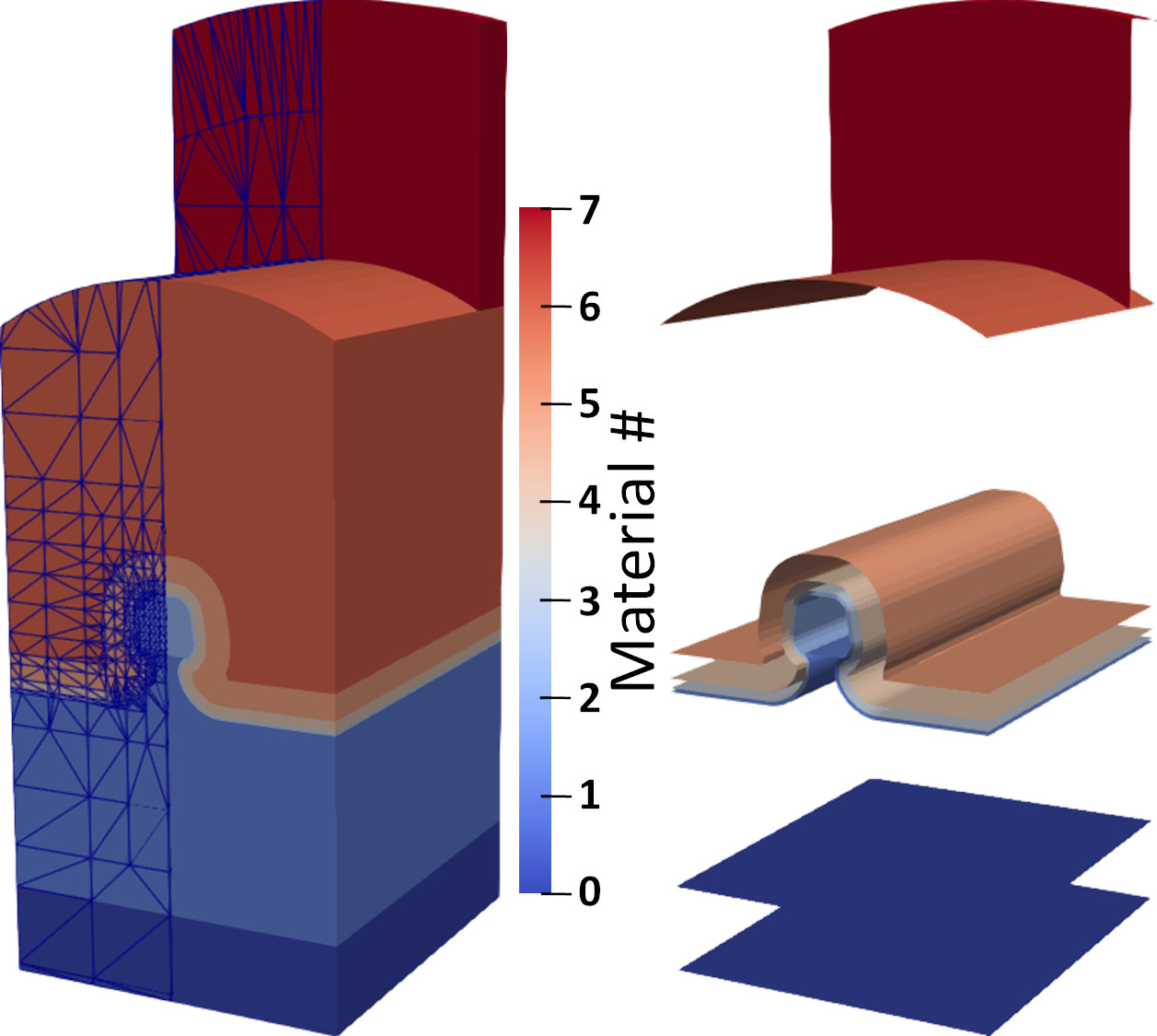
As part of this approach, which combines efficient continuum models with time-consuming and computationally expensive atomistic models that are highly important for understanding the chemical and physical properties of novel materials by using the former for the main simulation and only resorting to the latter when necessary, Head of Laboratory Lado Filipovic and his team are also looking for a solution to the central problem of existing state-of-the-art process simulators, which only define surfaces implicitly, making it very difficult to store material information: Such an implicit surface representation is to be combined with local material information - on the same grid and in the same data structure instead of having to repeatedly perform complex, error-prone and expensive conversions from implicit to explicit representations and vice versa, as has been the case up to now!
The researchers at the CD Laboratory for Multi-Scale Process Modelling of Semiconductor Devices and Sensors are thus not only making an important contribution to understanding new types of materials, but are also laying the foundations for the efficient manufacture of tomorrow's high-tech products.


