CD Laboratory for Single-Defect Spectroscopy in Semiconductor Devices
Head of research unit
Commercial Partner
Duration
Thematic Cluster

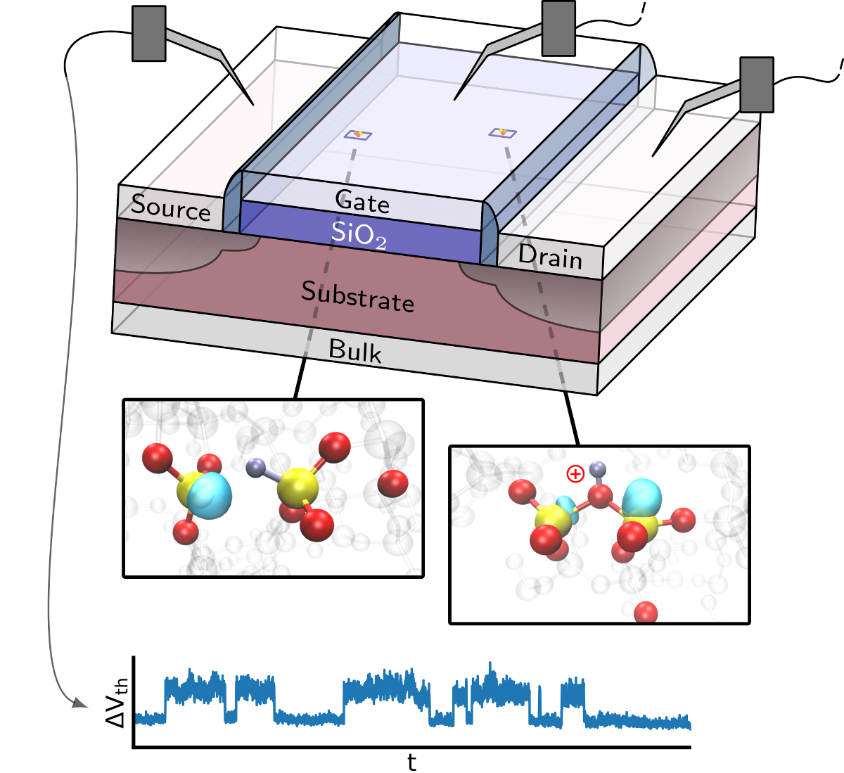
The lifetime and, above all, the performance of modern semiconductor transistors is decisively determined by individual electrically active defects in their atomic structure. Such defects can hardly be prevented during production and can also arise during operation. Research in the CD Laboratory for Single Defect Spectroscopy in Semiconductor Devices studies the influence of individual defects on the characteristics of new types of transistors and thus makes a significant contribution to their further development. Among other things, silicon carbide transistors, which are used in high-performance electronics, and low-noise silicon transistors for analogue amplifier circuits are studied in more detail.
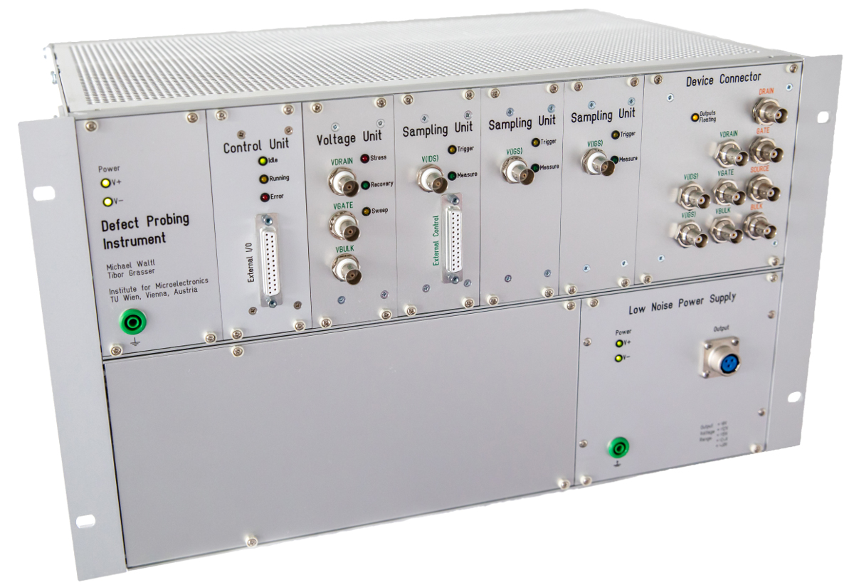
On the one hand, unsaturated bonds at the semiconductor/oxide interface (so-called interface states), but also defects in the atomic structure of the oxide and the semiconductor substrate, have a decisive influence on the performance of modern transistors. These defects are electrically active and can be generated under nominal operating conditions. They essentially lead to a reduction in the switching speed and to drift in the operating voltage, two of the most important parameters of semiconductor components. Although defect characterisation and modelling has received much attention in recent decades, the exact causes and physical properties are still not fully understood. So far, intensive investigations of state-of-the-art transistors only a few tens of nanometres in size have already provided an insight into the electrical behaviour of individual defects and their effects on component properties and service life. In this CD Laboratory, the complete investigation of defects faces two exciting challenges. Firstly, the investigation of technologies in which transistors only a few nanometres in size are not technologically relevant and therefore individual defects cannot be resolved by measurement. On the other hand, large structures have a large number of defects, which is also counterproductive for the detailed metrological detection of individual defects. However, in order to be able to detect individual defects in large structures at a microscopic level, research in the CD Laboratory is based on the so-called "zoom and scan" methodology, which for the first time enables single defect spectroscopy for non-scaled technologies. However, the measurements required for this are very complex and there is currently no suitable measuring system available. This will be developed and optimised in this CD Laboratory, among others, and then used in industrial practice. In addition to the metrological requirements, the physical modelling and interpretation of the measurement data represents another exciting challenge. Existing simulation models are used and further developed to explain effects such as low-frequency noise, hysteresis, drift of the operating voltage or oxide breakdown in addition to the electrical and transient properties of the individual defects. These models and tools go far beyond the current state of the art and will contribute significantly to the understanding and optimisation of semiconductor technology products.

Christian Doppler Forschungsgesellschaft
Boltzmanngasse 20/1/3 | 1090 Wien | Tel: +43 1 5042205 | Fax: +43 1 5042205-20 | office@cdg.ac.at

