CD Laboratory for Reliability Issues in Microelectronics
Head of research unit
Commercial Partner
Duration
Thematic Cluster

Influences on the reliability of semiconductor components and wiring structures are modelled and simulated. Generally applicable, scientifically based rules for the manufacture of such systems are developed.
The positions of microelectronic components, circuits or systems can fail due to changes in material properties. This risk is always present and also independent of the respective level of complexity. The aim of the research is to find innovative solutions that expand our understanding of this risk and that are not covered by current simulation software.
One focus of research is on electromigration reliability. This phenomenon refers to the current-induced transport of ions in conductor tracks, which destroys the tracks in the long term. In order to simulate this effect reliably, the effects of different designs of the wiring structure, material selection and microstructure are modelled.
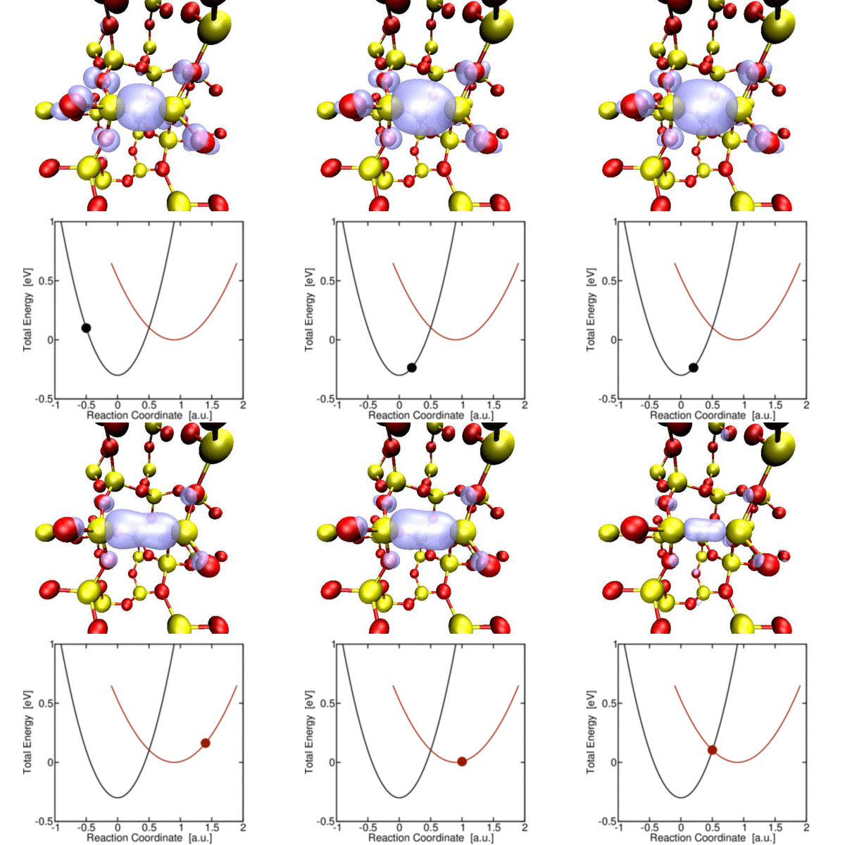
Furthermore, the influences of technological manufacturing processes (e.g. cleaning and oxidation) on the reliability of microelectronic components are modelled. The effect of mechanical stresses on complex structures with several layers is also analysed, as this can lead to separation from the individual layers (delamination) and cracks in such structures. Another area of work is the modelling of hot carrier degradation - where charge carriers overcome potential barriers and can damage components. It is a major obstacle to further miniaturisation and is therefore being researched in detail. Bias temperature instability (BTI), on the other hand, is a key reliability criterion for so-called MOS components. Therefore, one focus of the work is on the development of microscopic models of the defects that are responsible for BTI and for the dependence on time, temperature and electric field.
Together, these models and simulations will create rules that will enable increased reliability of semiconductor components.

Christian Doppler Forschungsgesellschaft
Boltzmanngasse 20/1/3 | 1090 Wien | Tel: +43 1 5042205 | Fax: +43 1 5042205-20 | office@cdg.ac.at

